This article is sponsored by Siemens Digital Industries Software. In this Voices interview, Engineering.com spoke with Michael Munsey, Vice President of Semiconductor Industry at Siemens Digital Industries Software, to discuss the importance of digital twins in semiconductor design and manufacturing. Munsey also shared insights on the role of software-defined products, new approaches for fab commissioning and operation, and the impact of artificial intelligence and machine learning on the semiconductor industry.
Editor’s note: This interview has been edited for length and clarity.
Engineering.com: Can you tell us about your background and what led you to your role as Vice President at Siemens Digital Industries Software?
Michael Munsey: After college, I began my career as a design engineer at IBM, where I worked on semiconductor development for IBM mainframes for many years. While working there, I became interested in EDA tools and methodologies. I had the opportunity to work in the EDA industry, where I joined Viewlogic Systems and worked there for several years.
I later joined a startup called Sente, which worked on RTL power analysis, long before power became a crucial aspect in the development of semiconductor devices. Then I went to Cadence, where I focused on design verification using Verilog and the entire functional verification suite. Then I moved to another startup that worked on semiconductor layout. I went back to Cadence to work on their enterprise solutions.
After this, I decided to venture out of the EDA industry, so I joined Dassault Systèmes, where I led their semiconductor industry and strategy. In this role, I learned about enterprise software and how to integrate semiconductor design and manufacturing within the enterprise software. Then I joined Methodics as Vice President for marketing, corporate strategy, and business development, and stayed with them through the Perforce acquisition of the company.
I joined Siemens in 2021 as Vice President of the Semiconductor Industry. I lead the semiconductor industry, focusing on EDA software, product lifecycle management tools, multi-physics simulation tools and AI platforms. All of these converge at the Digital Industries Software level, so I get to manage solutions that come across our entire portfolio of products.
How can semiconductor companies lean into digitalization and leverage the comprehensive digital twin for both semiconductor design and fab?
If you look at the semiconductor industry as a whole, the design and verification processes already leverage the digital twin. Engineers use advanced EDA tools to get digital design files that are handed off to the fab. We already have an industry that has done an excellent job on the design side of digitalization.
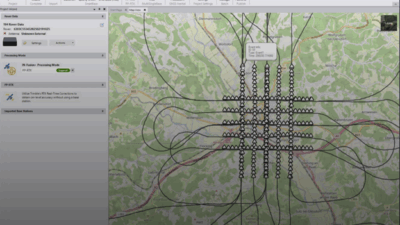
The gap exists on the manufacturing side. Unlike other industries that have embraced digital twins to simulate and optimize their production environments, semiconductors still rely heavily on real-time, physical experimentation, like running test wafers through fabs and bringing up new designs directly in real time manufacturing. This approach is both costly and time-consuming, especially at advanced nodes.
Now is the time to extend digitalization beyond design into semiconductor manufacturing. This means collaborating with fabs and equipment manufacturers to create digital twins of not only the chip designs but also the equipment and the fab processes themselves and use the digital design data as the foundation for simulating how a design interacts with a virtualized fab environment. Also, ramping up process nodes virtually so new designs can be brought up in a simulated fab before moving to physical production.
If the industry can achieve this, the payoff is substantial and will include significant time savings, reduced costs, faster time-to-yield and quicker time-to-volume of semiconductor devices. In short, bringing the digital twin to manufacturing is the logical next step for semiconductor companies to remain competitive at the leading edge.
What are the key benefits the comprehensive digital twin can provide for a business’s semiconductor ecosystem?
There’s a feed-forward and a feedback aspect to this. The first benefit, which I already mentioned, is doing things virtually. There are considerable cost savings because you are not wasting materials, electricity, and resources by doing this. Ideally, doing things virtually also allows you to do many more experiments for ramping up a process node.
A digital twin setup also gives semiconductor businesses the ability to optimize various critical processes. That’s definitely the feed-forward aspect of it. But there’s also feedback that enables shift left at the same time. For example, fabs can leverage real-time information from manufacturing to improve the PDKs continuously. This allows customers to make more manufacturable and yieldable designs up front that can get delivered into the fab.
What role do software-defined products play in the semiconductor industry, now and into the future?
When we talk about software-defined products, it is difficult to think about something that isn’t impacted by software today. If you look at the cars you drive, there is more and more software both in the way you interact with the vehicles and also behind the scenes in terms of how the car actually operates.
Unless you’re still building steam locomotives, chances are the product you are creating is somehow, some way, software-defined. What this really means is that there are numerous different products available, and with so much customization, the notion of having standardized compute platforms to build software-defined products on top of them is changing.
You rarely say, “I’m going to buy this microprocessor and build my platform around it.” What you see is customized processing platforms tailored toward the product and the software that needs to run on those platforms. That is changing the way software and semiconductors are developed.
The software and semiconductors are being developed in parallel. But software is being shifted to the left, where it’s starting to lead semiconductor development. Therefore, you need to ensure that the compute platforms can handle the software workload required to run on them when making those decisions. This is about making system-level decisions that are much more important.
How should companies in the semiconductor industry approach fab commissioning and operation?
In the past, the entire concept of building a new fab was to replicate one fab infrastructure to the next, with a few tweaks along the way. But when we consider the broader issues, such as sustainability and efficiency, there are more effective ways to build fabs. When you look at the macro impact of fab commissioning and operation, you want to make sure that it is being run as efficiently as possible. As a result, things like electricity and water usage, HVAC systems and filtration systems have a considerable impact.
The new approach would require digital analysis for building fabrication facilities, supported by real-time, detailed information about the projects within these fabs. This strategy will make sure that we’re building and commissioning green fabs that are energy-efficient and resource-optimized.
How are artificial intelligence and machine learning impacting the semiconductor industry?
We’re looking at AI from multiple angles. First, the features built into products need to be supported by the underlying semiconductor designs. Second, the impact of actually running AI workloads on those products. And third, how AI itself is transforming the way we design and manufacture those products.
So, it’s pervasive throughout the entire industry. The design and verification tools are much more advanced than they were even a year ago because of the AI algorithms that are being integrated within them. On the manufacturing side of things, it gives the ability to understand the way fabs operate and be able to have intelligence at the industrial level.
You could query the AI platform, asking questions on the operability of the manufacturing equipment, potential errors and fixing solutions. AI solutions will enable factory floor operators to automate the actual fixing of mistakes in the manufacturing facilities. We’re seeing things changing at an exponential rate, all the way from design and verification to manufacturing. Ultimately, we see AI having drastic effects that are going to allow us to significantly improve the way we design, verify and manufacture semiconductors moving forward.
To learn more about how Siemens is impacting the semiconductor industry, visit siemens.com/us/en/industries/semiconductors.